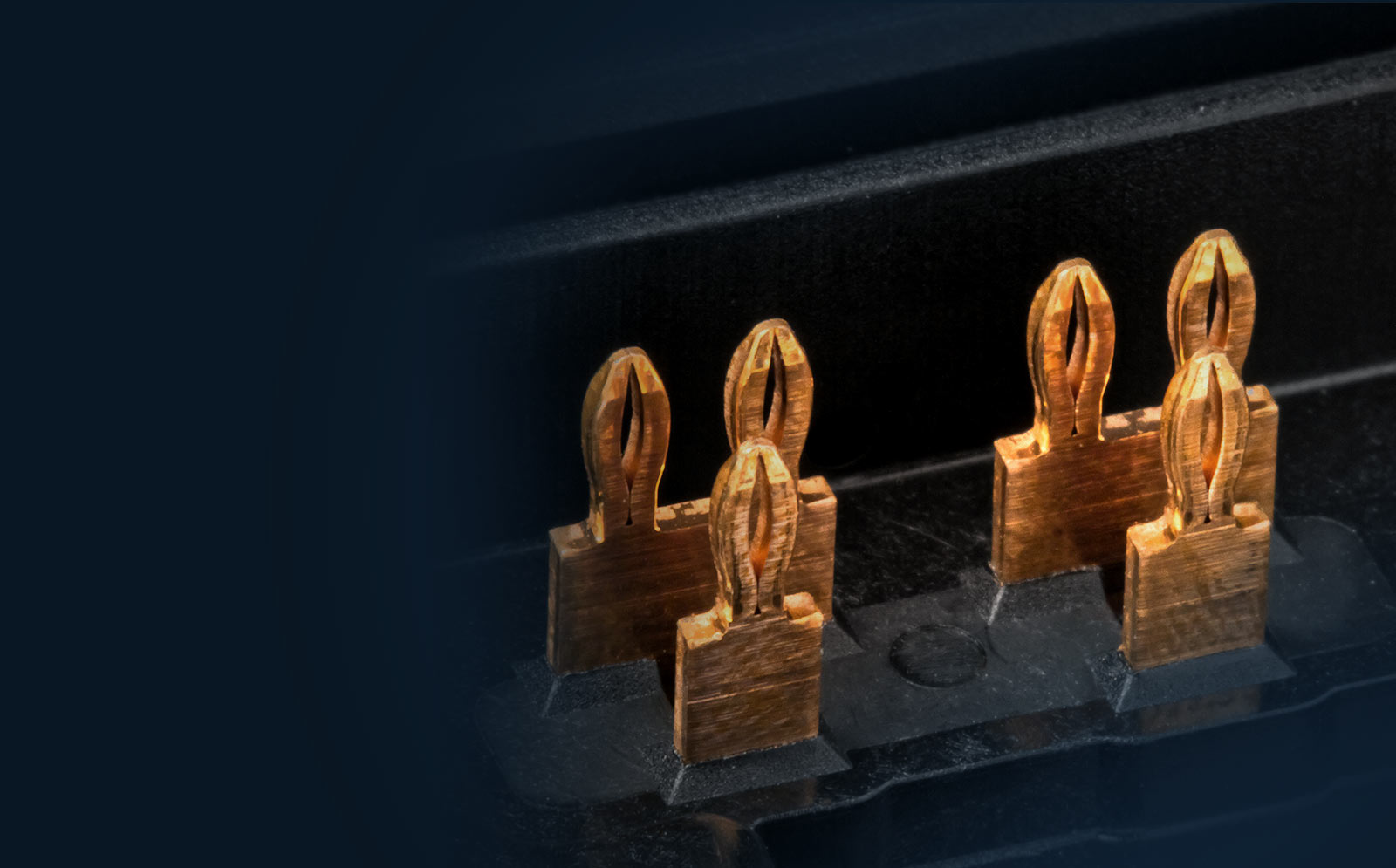
A press-fit zone with particular flexibility
We can give you broad-ranging design flexibility in terms of material selection, material thickness, material strength and adaptability to your specific needs and technical requirements. Made to measure exactly to the customer's needs.
Providing BIZON® press-fit technology, ZETKA offers an innovative solderless contacting system for all requirements in the automotive supply industry, electrical engineering, power electronics and any other application where secure contact connection to a printed circuit board or metal plate defines the quality of the final product.
Solder-free, robust and secure
This press-fit technology is a solder-free, robust, secure electrical connection technology in which preferably elastic, formable pins are connected into metallised (copper-plated) printed circuit board holes with defined dimensions at a defined speed using a press-fit facility. This produces a permanent gas-tight mechanical and electrically low-resistance connection (cold welding) at the contact surfaces between the press-fit pin and the hole's metallic inner wall. The unique spring properties of the BIZON® press-fit contact prevent any damage to the printed circuit board if the press-fit process is carried out correctly, thereby preventing delamination (whitening) and tearing of the inner layers.
Press-fit technology for high-current applications with optimised maximum contact surface
The key aspect and major benefit of BIZON® press-fit technology lies in providing the greatest possible square cross-section with accurate self-centring in the PCB hole. The conductor cross-section this achieves is approx. 72% of the hole cross-section, permitting a high electrical strength per contact. With its four defined contact areas, each BIZON® contact provides maximum contact surfaces and, as such, outstanding and secure contact properties. This provides the capability of safely handling several hundred amperes with standard 75 µm printed circuit boards (70 A per contact, hole 2.0). This is a key cost advantage for any high-current application.
Depending on the application, you can avoid unnecessary cost and time-intensive surface finishes in the press-fit zone by using bare BIZON® contacts. This prevents the formation of whiskers and tin chips which can lead to failure of the entire assembly down the line. The contact can be produced in any size and sheet thickness of any material you choose. Exact harmonisation with your particular application can avoid the need for expensive special materials by using standard materials. Let us show you the options and limits.
Contact variations and application areas
- Stamped BIZON® contacts – open or closed tip – in strip form or individual
- Sheared BIZON® contacts for extremely close contact spacing – in strip form or individual
- Shielding housing – with multiple pins
- Stamping grids - with complex geometries on the strip or in trays
- Busbars – for feeding high currents into the printed circuit board
- Pre-stamped strips – with standard zones for small batches or prototypes
- Special applications tailored exactly to customer requirements
Benefits
- Reliability more secure and longer-lasting than a conventional solder joint
- Space-saving in application with optimum use of package space (design to cost)
- Cost edge in processing and purchasing
- Simplification in processing as no need for complex process steps
- Process reliability thanks to the monitored BIZON® contact production process
- Material compatibility: compliance with automotive specifications (e.g. IMDS, CAMDS, RoHS, Reach)
- Mixed assembly on a printed circuit board – through variable tip height
- No collapsing – a major drawback of the needle-eye pin has been eliminated
- High plastic deformability – low spread of press-in force
- Maximum elasticity – double spring length, utilisation of PCB relaxation, short printed circuit board overhang
- Compliant with standards meets the requirements of DIN EN IEC 60352-5, IPC 9797
- BIZON® technology benefits from 40 years of experience in connecting systems and standardisation expertise
Electrical and mechanical properties
- High electric strength with minimum need for space
- Four contact edges with maximum contact surface
- Material thicknesses from 0.2 mm to 2 mm
- Low press-in force from a high level of flexibility
- Low contact resistances
- High retaining forces from cold welding
- No whisker formation and tin chips with bare press-fit zones
- Disassembly possible simply by pressing out
- Temperature range from -40°C to 180°C, also making them suitable for use at extremely high and low temperatures.
Distribution and direction of force into the printed circuit board

Our micrographs show the cross-section in the printed circuit board hole using the example of a BIZON® contact made of 0.8 mm material.
Four symmetrically distributed, widely spaced and defined contact surfaces mean calculable contact pressure.
- Four equal radial contact forces provide good self-centring ability and symmetrical support – the contact adjusts to the hole.
- No torque, no tangential movement and no bending in conjunction with extremely small hole diameters.
- Force is distributed over the full area which means no force summation and no elongation of the printed circuit board (minimising the risk of damage to the printed circuit board).
- Distributing the compressive forces over four areas reduces load on the printed circuit board to 25% per contact point. This results in hardly any deformation and sagging of the printed circuit board. And provides maximum possible protection for SMDs.
Material thickness / strip thickness and hole table
Overview
| Sheet thickness (mm) | Pin dimensions (mm) | ∅ - range of finished hole LP (mm) | for stamping reasons smallest stamping (mm1) |
| 0,2 adapted 2) | 0,20 x 0,24 | 0,30 – 0,38 | 0,81 |
| 0,4 adapted 2) | 0,40 x 0,50 | 0,55 – 0,65 | 1,30 |
| 0,6 | 0,60 x 0,60 | 0,80 – 0,90 | 1,20 |
| 0,64 | 0,64 x 0,64 | 0,90 – 1,00 | 1,30 |
| 0,64 adapted 2) | 0,64 x 0,80 | 1,00 – 1,10 | 1,45 |
| 0,8 | 0,80 x 0,80 | 1,05 – 1,15 | 1,60 |
| 0,8 adapted2) | 0,80 x 1,20 | 1,40 – 1,55 | 2,00 |
| 1,2 | 1,20 x 1,20 | 1,52 – 1,67 | 2,40 |
| 1,2 adapted2) | 1,20 x 1,50 | 1,90 - 2,05 | 2,70 |
| 1,5 | 1,50 x 1,50 | 1,90 - 2,05 | 3,00 |
| 2,0 | 2,00 x 2,00 | 2,70 | 4,00 |
All dimensions are in millimetres
¹ For single contacts (plug-in module), application pitch is determined by the application and safety distances.
² The contact is adapted to historically standard, larger or production-related hole diameters.
Qualification
Manufacturability analysis, development, prototypes and production.
ZETKA is not only the manufacturer of the BIZON® press-fit zone, we are your development partner and consultant before a component drawing is even produced. In the project phase of the product development process we provide the specifications for the main influencing parameters, such as base material, press-fit zone geometry, current strength and fitting situation in the final application. The resultant parameters are fed into the product drawing and then permanently monitored in volume production. In the test laboratory, the main key data and requirements under DIN EN 60352-5 as well as your requirements can be tested and validated in the course of volume production. We have the inspection and measuring equipment required to do this. Inspection is carried out using exactly toleranced test PCBs with minimum and maximum tolerances or, if you wish and also our preferred option, your volume-produced circuit boards This way, we can ensure that your products perform in the proper way.
- Visual inspection
- Dimensional inspection
- Press-fit and press-out force with appropriate rest period by means of a tensile testing machine
- Generation and evaluation of microsections
- Measurement of contact resistance
Patents, licences and safety
BIZON® contacts are protected by several patents, have been proven many times over in the field and have been well established on the market for many years. The BIZON® brand is protected under number 017570698. Patents: EP 1 754 285, US 7,891,992, DE 10 2017 119 432, US 10,153,567
For further information, please go to www.bizon-kontakt.de
Your career at Zetka
ZETKA is a company of the FIR Group, operating successfully both nationally and internationally, and offers jobs with prospects. Whether in development, production, service or sales – we still have a lot to do and are always looking for good people to strengthen our team with a targeted approach.
Training and placements
Cross-border exchange possible


